Speaker
Description
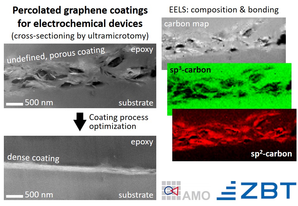
Energy devices are commonly assembled from multiple functional components. To gain fundamental understanding of the microstructure-property relations between individual components, their degradation and failure mechanisms and to enable characterization/optimization cycles through transmission electron microscopy (TEM), it is desirable to prepare electron transparent cross sections of entire devices or of as large sections of a device as possible. Since most TEM specimen preparation techniques are optimized for specific material classes, preparing TEM samples of devices consisting of different materials may be difficult. Therefore, TEM sample preparation is often preceded by the disassembly of a device down to individual components rendering an investigation of relations between the individual components impossible.
Ultramicrotomy as a cross-sectioning technique can solve these problems as it can generate ultra-thin, electron transparent cross sections tens to hundreds of micrometers in size, which is typically larger than the structure sizes in modern, micro- and nanostructured devices. As no ionizing radiation is used, artifacts due to beam damage are avoided.
We demonstrate the capabilities of ultramicrotomy in conjunction with advanced TEM characterization down to the atomic scale, when high quality, thin samples are provided. Examples include devices like complex PEM fuel cells and battery parts. The achieved thickness of the cross sections is commonly below 50 nm, which enables routine (atomic-resolution) imaging by various techniques, each providing their unique image contrasts, but also the application of various spectroscopic mapping techniques. This renders TEM ideally suited to investigate the interfaces of individual layers and components in terms of their morphology and contact as well as the systematic identification of their composition and chemical bonding states.
Part of this work was performed at the Micro-and Nanoanalytics Facility (MNaF) of the University of Siegen.
| Speaker Country | Germany |
|---|